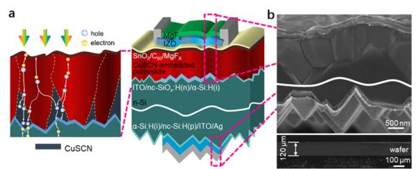
An international research team has fabricated a 1 cm2 perovskite-silicon tandem solar cell that utilizes a top cell based on a perovskite absorber integrating inorganic copper(I) thiocyanate (CuSCN).
“A co-deposition strategy of CuSCN and perovskite is firstly developed to solve the key technical challenge to fabricate perovskite top cell on textured silicon bottom cells,” the research’s corresponding author, Xingbo Yang, told pv magazine. “Besides, the inorganic CuSCN is also applied in perovskite/silicon tandem solar cells for the first time and the resultant devices demonstrate extraordinary light and damp-heat stabilities.”
The researchers explained that they decided to build the top cell without a hole transport layer (HTL), as HTLs used in top cells for tandem devices usually suffer from defects caused by non-conformal deposition or de-wetting. They deposited the perovskite precursor ink with CuSCN directly on the recombination layer made of indium tin oxide (ITO) of a 24.42%-efficient heterojunction (SHJ) bottom cell.
“Our approach here has been confirmed to form local hole-collecting contacts by embedded CuSCN in device, resulting in a different device structure from that of a common and classic p-i-n configuration based on a thin self-assembly monolayer (SAM) on recombination layers like ITO,” Yang further explained.

The scientists build the top cell with an ITO substrate, passivating contacts based on silicon monoxide (poly-SiOx), the CuSCNE-embedded perovskite absorber, a tin oxide (SnO2) layer, a buckminster fullerene (C60) electron transport layer (ETL), and an anti-reflective coating based on magnesium fluoride (MgF2).
In this cell configuration, the CuSCN phase embedded at perovskite grain boundaries acts as both an efficient local hole-collecting contact and a defect passivator. “We verified that CuSCN aggregates at grain boundaries of the buried perovskite surface at a certain depth, forming local hole-collecting contacts for efficient hole transfer and grain boundary passivation,” the academics stressed.
Tested under standard illumination conditions, the tandem device achieved a power conversion efficiency of 31.46%. It was also able to retain 93.8% of the initial efficiency after about 1,200 h of maximum power point tracking at 45 C, and 90.2% after over 1,000 h of damp-heat testing at 85 C and 85% relative humidity.
“To be commercially valuable, the scale-up of tandem devices has been verified with an aperture area of 4 cm2 realized by both spin-coating and blade-coating, demonstrating competitive aperture power conversion efficiencies of 28.14% and 25.23%, respectively,” Yang added. “It indicates great scalability and universality of our co-deposition method.”
The device was introduced in the study “Efficient and stable perovskite-silicon tandem solar cells with copper thiocyanate-embedded perovskite on textured silicon,” published in nature photonics. The research team included scientists from Soochow University, Zhejiang University, and the Hong Kong Polytechnic University in China, as well as the King Abdullah University of Science and Technology (KAUST) in Saudi Arabia and Chinese PV production equipment provider Maxwell Technologies.
This content is protected by copyright and may not be reused. If you want to cooperate with us and would like to reuse some of our content, please contact: editors@pv-magazine.com.

